What it is
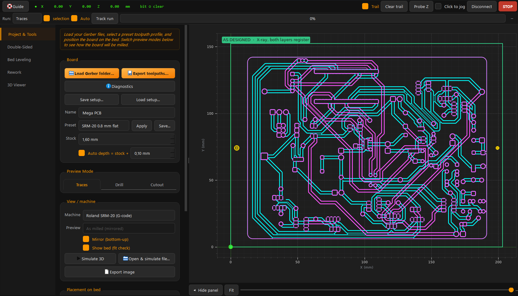
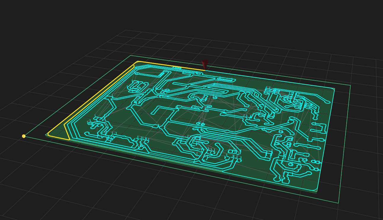
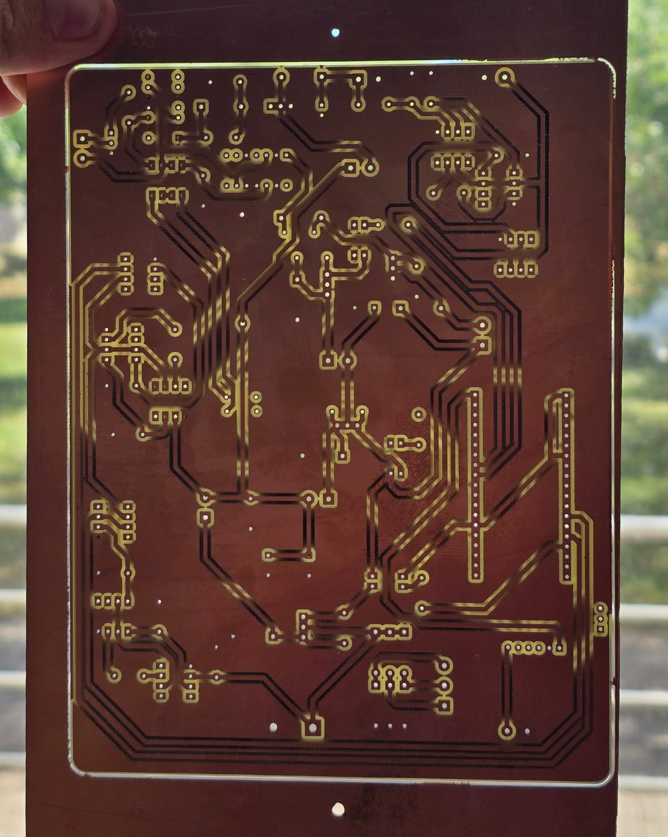
The Roland SRM-20 is a small desktop CNC mill that can isolation-route PCBs — cut the copper away from around the traces instead of etching it. The stock toolchain for that is slow web tools (mods.io) or fragile wrappers around FlatCAM. SRM-CAM is my replacement: one Python package with both a GUI and a CLI that takes KiCad Gerber + Excellon files and produces the machine code the SRM-20 actually runs. It previews the cut in 3D, probes and compensates for a warped board, handles double-sided registration, and re-cuts individual failed traces without regenerating the whole job.
It’s the tool that drives the CNC half of my dorm-room PCB fabrication line, and it’s used by other students at the DTU Ballerup fab lab. It’s also the project I’m proudest of — the one I’ve poured the most hours into, a lot of them late nights and even between classes at school. If you only read one page on this site, I’d want it to be this one.
Problem / motivation
Milling a PCB sounds like a solved problem until you try it. A board is never perfectly flat — a 130 µm bow over 50 mm is normal — and an isolation cut only 0.1 mm deep will skip copper in the low spots and gouge the substrate in the high spots. Double-sided boards need the two faces to line up to under 0.1 mm after you flip the stock. And the SRM-20 deliberately hides the machine state behind a proprietary control panel. I wanted a tool that treated these as first-class problems instead of hoping the board was flat and the operator was lucky.
Architecture / approach
The package (gerber2rml) is split into an engine that has no GUI dependencies and a PySide6 front-end on top:
- Parsing — Gerber traces and Excellon drills into an internal geometry model.
- Toolpath engine — isolation offset, drill, and board cut-out paths; ramped lead-in; Liang–Barsky segment clipping for region rework.
- Registration — dowel-pin or fiducial-based two-sided alignment (closed-form 2D Umeyama similarity fit).
- Leveling — a probed height map (plane fit for tilt, bilinear for bow) that warps every cut’s Z in machine coordinates.
- Backends — G-code (
.nc, recommended) or Roland’s RML-1 (.rml). - Hardware — an Arduino Uno running a custom SPI probe sketch that talks to the SRM-20’s official remote header.
The engine is heavily unit-tested (54 test files, ~6k lines of tests — roughly a 42% test-to-code ratio on a geometry- and GUI-heavy project), with GUI tests running headless via QT_QPA_PLATFORM=offscreen.
What went wrong and how it was diagnosed
This is where the project actually lives. A handful of the concrete failures:
Dowel holes came out 0.4 mm undersize. Double-sided boards wouldn’t re-register after the flip — the alignment pins physically wouldn’t seat. Measured holes were ~2.7 mm where 3.1 mm was commanded. The cause is that the SRM-20’s internal compensation undershoots on interpolated (circular) cuts. I dialed in per-pin clearance compensation empirically with a swept fit-test coupon — one drill job with holes stepped across a range of diameters, cut once, pick the snug one by hand — landing on +0.20 mm for the 3.1 mm pins and +0.15 mm for the 1.9 mm pins. The offsets are non-linear, which is why each pin size needed its own. Registered boards then held to under 0.1 mm.
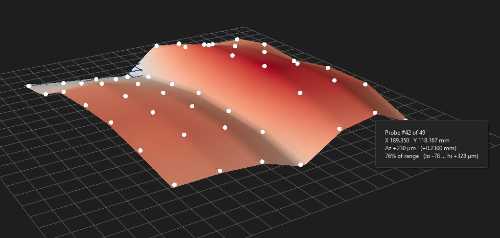
“Leveling” made the middle of the board worse. After probing a board with the first-generation 3-point routine, center traces cut shallow and corners cut deep. A test board measured 130 µm of bow. The bug was that three points can only ever fit a plane — the routine was correcting tilt while assuming the board was flat, when the real error was curvature. Fixed by probing a full grid and doing bilinear interpolation (HeightMap.from_grid auto-selects plane vs. bilinear by point count), plus a two-phase probe: a fast coarse raster at 25 µm steps, then a fine re-probe of only the last ~1 mm at the machine’s native 10 µm resolution.
Endmills snapped on first contact with copper. The SRM-20 has no S word — spindle RPM is a front-panel slider, and M3 starts the spindle concurrently with motion rather than waiting for it to spin up. So the bit was hitting copper mid-acceleration. Two independent fixes: a G04 X2. dwell emitted after every M3 so the spindle reaches full speed before any motion, and a ramped lead-in (engine/leadin.py) that descends to full depth over the first ~1 mm of the cut path instead of plunging vertically. The G-code parser had to learn to skip G04 lines so the simulator didn’t read the dwell’s X2. as an X coordinate.
V-bit traces came out wildly inconsistent. Engraving 0.2 mm SMD traces with a V-bit on an unleveled bed gave visibly uneven widths. The geometry explains it: for a V-bit, width = tip + 2·depth·tan(θ/2), so dW/dD ≈ 0.5–2.0 µm per µm of depth error — a 25 µm height error becomes a 13–50 µm width error. I flipped the tool model from depth-first to width-first (operator sets target width, depth is back-solved) and made the preflight check refuse to run a V-bit job without bed leveling enabled, because on a V-bit the leveling isn’t optional.
Results
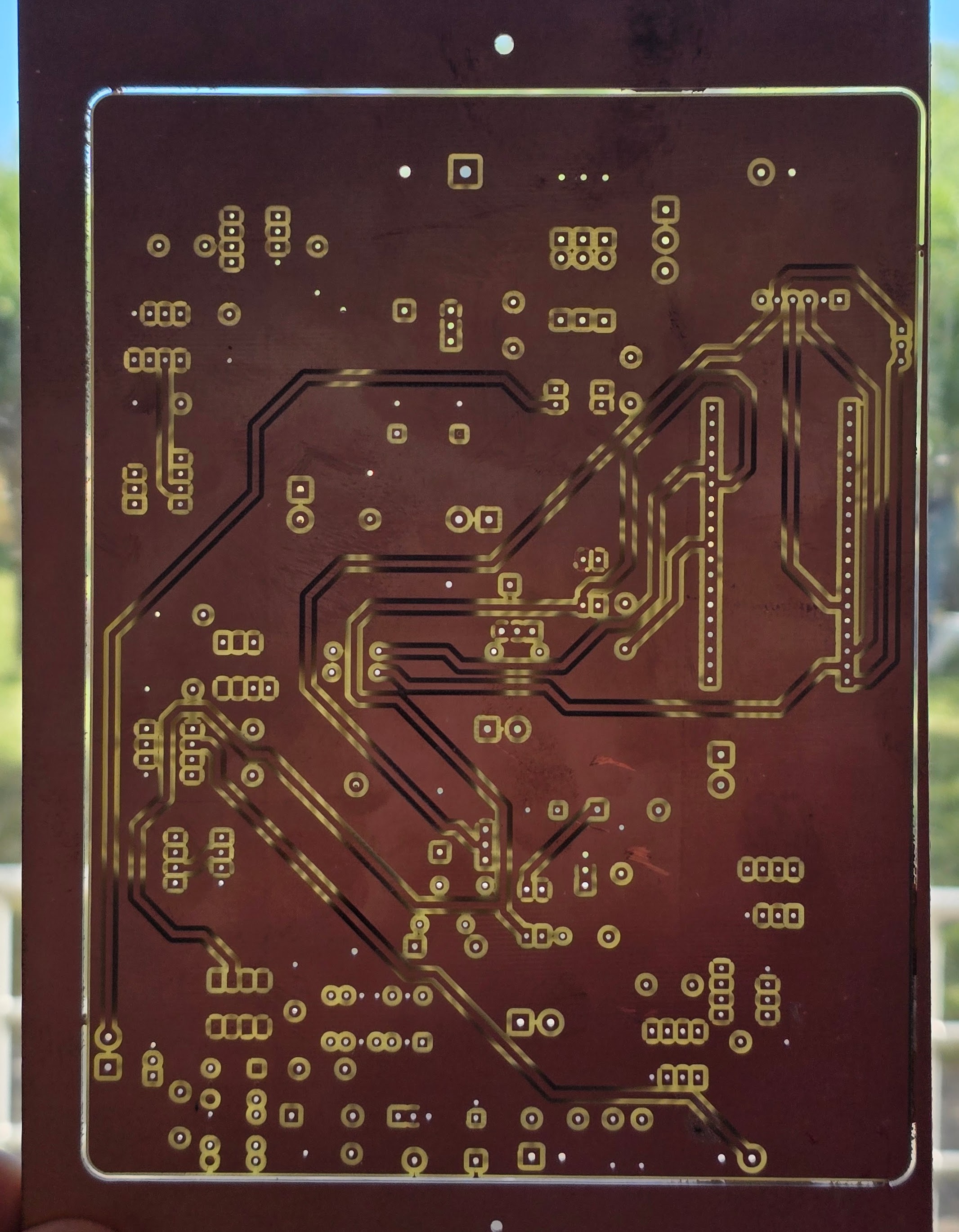
- Full KiCad-to-milled-board pipeline working: traces, drills, cut-out, double-sided.
- Double-sided registration holding to <0.1 mm after flip (dowel and fiducial methods).
- Bed leveling handles real board bow (validated against a 130 µm bowed board).
- Grid probe of a typical board completes in ~5 minutes.
- 334 passing tests at last count; ships as a Windows installer built in CI.
Tools & skills demonstrated
Reverse-engineering an undocumented machine interface (SPI probe over the SRM-20 remote header), computational geometry (segment clipping, similarity-transform fitting, height-map interpolation), G-code/RML generation, Arduino firmware, a PySide6 desktop app with an embedded 3D view, and disciplined testing on a hard-to-test codebase.